Dispelix and Eulitha co-develop novel nanofabrication process for high-fidelity nanostructures
Dispelix, a technology leader in diffractive waveguide technology for augmented reality (AR), and Eulitha, a global leader in advanced lithography solutions, have successfully demonstrated a novel nanofabrication process. This new process enables the production of high-fidelity nanostructures using Displacement Talbot Lithography (DTL) and a three-layer stack with dry etching.
Diffractive waveguides are the leading technology for augmented reality displays, enabling precise control of light through nanoscale gratings etched into thin films. These gratings are fabricated using typical semiconductor manufacturing processes such as thin film deposition, lithography, and etching.
The grating layer is deposited onto the substrate first, followed by an etching or hard mask. Lithography is then used to define the features of a resist mask on top of the hard mask. Dry etching is then used to transfer the structures from the resist into the hard mask and finally to the grating layer.
High structural fidelity in diffractive waveguides depends on precise lithography and etching. DTL is an optical lithography technique that delivers the necessary high-resolution patterning, enabling seamless fabrication of numerous waveguides in a single exposure. DTL offers significant advantages in terms of reliability, scalability, and cost-effectiveness. After lithography, the etching process must accurately transfer these patterns through a thin hard mask – usually a layer of chromium of a few tens of nanometers – into the grating layer. While thin hard masks are ideal for standard designs, advanced waveguides with tall or slanted gratings, which are typically etched using reactive ion beam etching, require thicker masks. In these cases a thin resist layer is not sufficient to ensure high structural fidelity of the gratings.
To address this challenge Dispelix and Eulitha have co-developed a process that leverages the advanced capabilities of DTL. The breakthrough lies in the use of a three-layer stack that allows for the successful etching of thick hard masks – up to 100 nm of chromium – while maintaining structural fidelity and precision. This advancement is critical for enabling the fabrication of slanted gratings via reactive ion beam etching, which traditionally consumes thin hard masks too rapidly for optimal results.
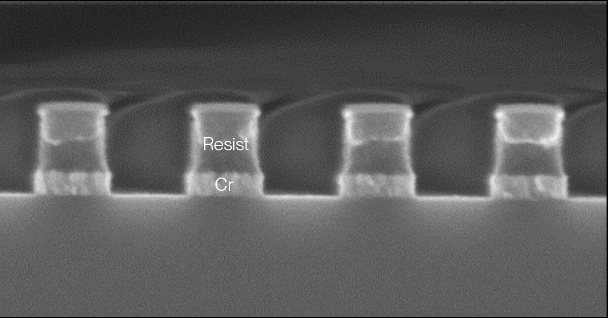
Figure 1: Scanning electron microscope cross-section of a grating etched on a 50 nm thick chromium layer. Note that the residues of the resist layer are still in place.
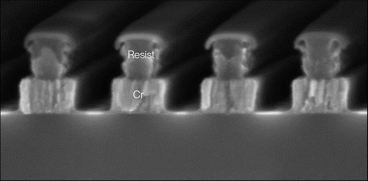
Figure 2: Scanning electron microscope cross-section of a grating etched on a 100 nm thick chromium layer, also with the residues of the resist still in place.
“This jointly developed process allows the production of highly sophisticated diffractive waveguide solutions with unmatched structural fidelity,” says Ismo Vartiainen, CTO of Dispelix. “This not only enhances AR display performance but also opens new possibilities for other nanophotonic applications, such as metalenses or metagratings, where the grating layers are very thick and require robust etching masks.”
About Dispelix
Dispelix develops and delivers transparent waveguides for enterprise and consumer augmented reality (AR) devices. Our advanced waveguides function as see-through displays in AR devices, fusing the real and virtual worlds within the user's field of vision. We are a trusted and visionary partner for the industry leaders in AR, enabling them to redefine the form, function, and feel of AR devices.
About Eulitha
Eulitha provides advanced lithography equipment and services, specializing in high-resolution, periodic patterning solutions. Eulitha’s proprietary Displacement Talbot Lithography (DTL) technology enables seamless patterning down to ~50 nm half-pitch over large areas (140 x 140 mm), with exceptional depth of focus suitable for non-planar substrates. Eulitha’s systems offer highly reliable, repeatable optical lithographic exposures at a cost-effective price point. The company is headquartered near Zurich, Switzerland, with offices in China and the United States.